


ITEM SPECIFICS
-
Brand
Model I-View 1000Unbranded
-
origin
Republic of Korea
-
Size(Capacity)
Unknown
PRODUCT DESCRIPTION
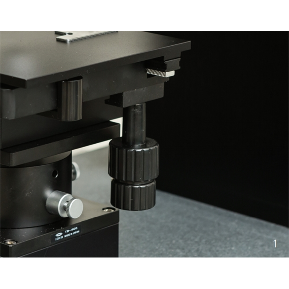
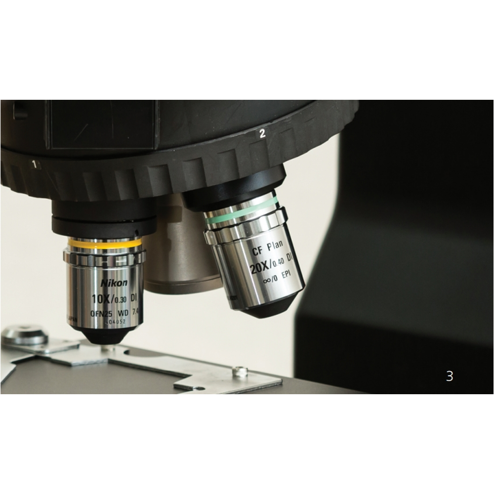
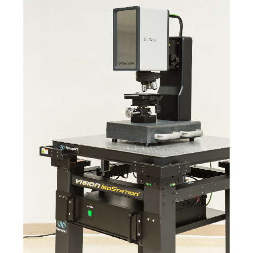
noncontact 3D measuring measures the surface shape of a fine pattern with a height of 1nm ~ 10mm using light interference. Compared to AFM or contact profiler, it is possible to realize a wide measurement area and high speed, and it has a powerful advantage of measuring 3-dimensional shape on the surface without damaging the measurement object.
==Semiconductor==
Stud Bump : Diameter, Height, Volume, Roughness, Angle
CMP : Warpage, Roughness
CVD : Roughness
Wafer : Warpage, Scrach, Roughness
==LCD/OLED==
Photo Space : Diameter, Height, Width, Volume
RGB : Thickness, Roughness, BM Thickness
TFT Pattern : Height, Width, Roughness
BLU : Shape, Width, Height, Angle, Roughness
Ink Jet : Width, Height, Angle, Roughness
Glass : Defect Form/Width/Height,
OLED : Thickness & Shap
==PCB Substrate==
Substrate (Pad, Trace, Space, Anchor, Land, Ball Pad, Via Hole, Dimple, SR)
: Height, Width, Depth, Dia, Thickness, Volume, Roughness, Roundness
BGA : Ball Height, Dia,Coplanarity
==Etc==
MEMS : Height, Width
Precision machine part : Roughness
Laser Marking : Depth, Volume
Inkjet : Volume, Height, Area
Micro Lens : Curvature
RFID : Height, Width, Roughness
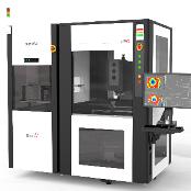
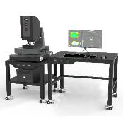
==Hardware==
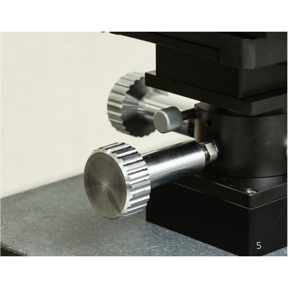
- Equipment
- Isolation Table
- Table
- Computer
- Monitor
==Software==
- Surface View(Opperator Program)
- Surface MAP (Analysis Program)
R&D CERTIFICATE
-
- ISO Certificate
- ISO
- 20150824
- 인증서보기
PAYMENTS DETAILS
- Telegraphic Transfer : T/T
- Name : Ho Hwan Kim
SHIPPING
- 65 Sinilseo-ro 85beon-gil, Daedeok-gu, Daejeon (34325)
The person in charge
Ho Hwan KimAddress
65 Sinilseo-ro 85beon-gil, Daedeok-gu, Daejeon (34325)
-
- Business Type :
- Manufacturer
-
- Main Product :
- SURFIEW Premium (Surfiew4000)
-
- Established :
- 2015-02-24
-
- Total Annual Revenue :
- 3~5 million (KRW)
-
- Total Employees :
- Less than 5
R&D CERTIFICATE
-
- ISO Certificate
- ISO
- 20150824
- 인증서보기
COMPANY ENVIRONMENT


Please suggest a variety of your ideas such as design, impact, enhancements, etc
Please enter the text on the left image to prevent automatic input.
0 / 4000
CUSTOMER REVIEWS (0)

TRADE EXPERIENCE
-
- Total revenue
- 3~5 million (KRW)
-
- Total export revenue (previous year in USD)
- 2
-
- Number of foreign trade employees
- Less than 5
COMPARISON TO SIMILAR ITEMS more
- No Items
- supplier level
- MEMBER
- GL-Tech Co.,Ltd Seller's Store
- Seller's Store url
- Response Level
★ ★ ★ ★ ★

- Supplier Level
★ ★ ★ ★ ★
- Transaction Level
★ ★ ★ ★ ★